An RF engineer orders chemically etched lead frames for a 100,000-unit QFN program because etching requires no tooling and delivers parts in one week — six months into production, the $0.18 per-frame cost burns through $18,000 when a progressive die at $30,000 would have dropped the per-part cost to $0.04 after amortization. The zero-tooling advantage evaporated at 10,000 pieces, but the etching vendor was locked into the annual contract.
This comparison breaks down the tolerance boundaries, volume thresholds, and material constraints that determine whether stamped electrical terminals or chemically etched lead frames deliver the lower total cost for your specific program parameters.
Read on for the full comparison.
When Progressive Die Stamping Wins
Three-Dimensional Forming Capability
Stamping can form three-dimensional features —bends, lances, embossments, and coining —that chemical etching cannot produce. An etched lead frame is fundamentally a two-dimensional part: the etchant removes material in the X-Y plane but cannot create a Z-axis bend, a raised contact dome, or a coined surface flatness improvement. Every 3D feature on an etched part requires a secondary forming operation —a separate bending or coining station that adds process cost and handling complexity.
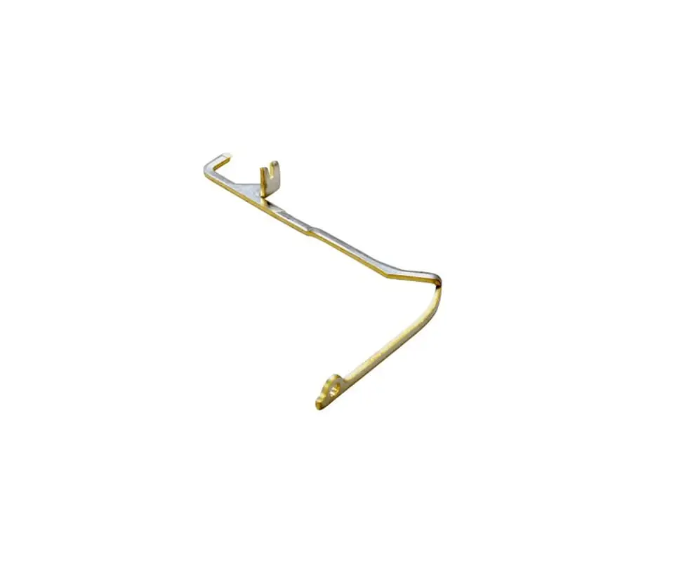
For stamped electrical contacts that require a spring-loaded contact beam with a specific normal force, the bend forming happens in the same progressive die that pierces the blank profile —no secondary operation, no part handling between processes. Kravzik‘s in-house progressive die tooling capability enables integrated piercing, coining, forming, and even in-die staking of secondary components within a single die set for custom metal terminals that ship assembly-ready from the press exit.
Plating Integration and Surface Preparation
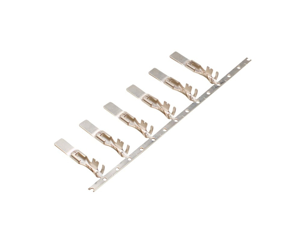
Progressive die stamping leaves terminals attached to their carrier strip —a continuous web that feeds directly into reel-to-reel selective plating lines. This integrated workflow eliminates part handling between stamping and plating, preserves surface cleanliness, and enables selective precious metal deposition on the contact zone alone. Etched lead frames exit the process as loose individual parts or panel arrays that require singulation before plating, introducing handling steps and surface contamination risk between etching and plating operations.
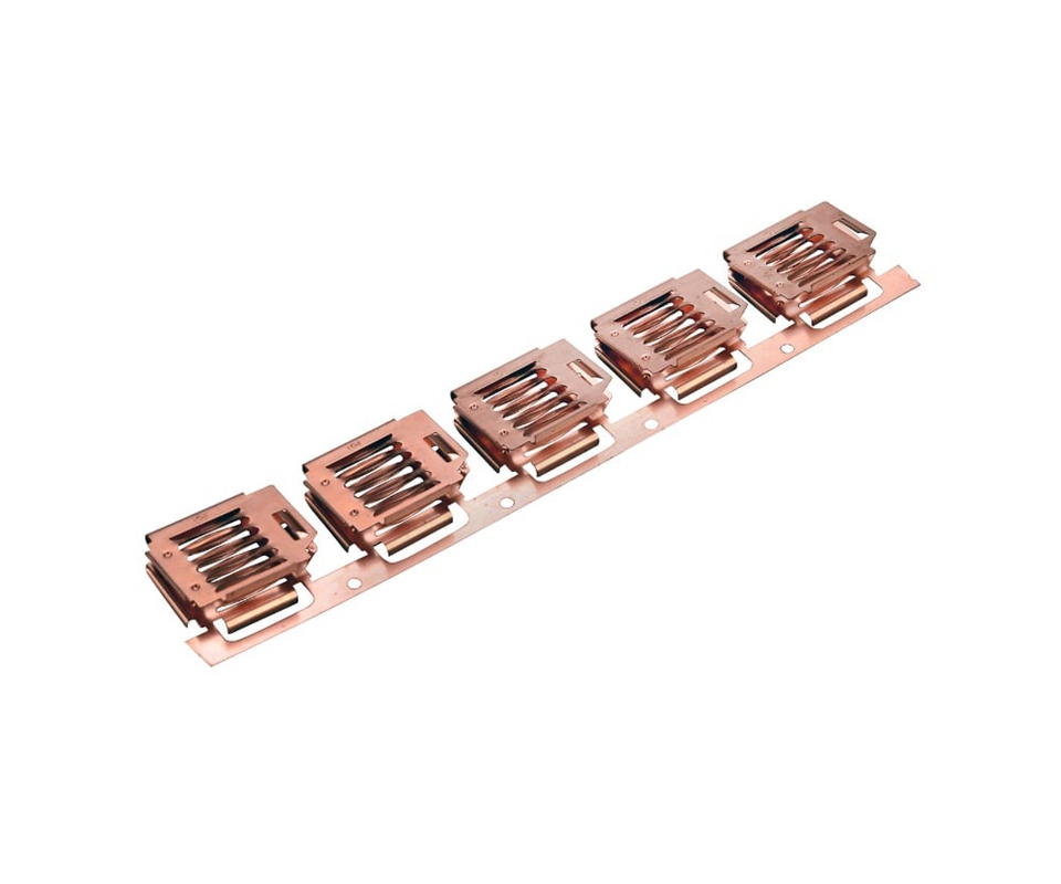
For terminals requiring selective gold or silver plating on the contact beam, the plating logistics advantage translates to $0.003 to $0.010 per part in handling cost savings for stamped-and-selectively-plated parts versus etched-and-bulk-plated alternatives. Kravzik operates full in-house plating lines adjacent to the press floor, accepting terminals directly from progressive die presses in a closed-loop process that eliminates the 3-to-5-day transit time that outsourced plating introduces for etched parts. This integrated workflow is especially critical for electrical component metal stamping programs where surface cleanliness directly affects wire bond pull strength and solderability.
[Verdict]: If your annual production volume exceeds 50,000 units and your terminal geometry requires three-dimensional forming features or integrated selective plating, choose progressive die stamping.
When Etched Lead Frames Win
Zero Tooling: Prototype and Low-Volume Programs
Chemical etching requires no hard tooling. A phototool —a film artwork generated from CAD data —costs $500 to $2,000 and produces in 3 to 5 days. A progressive die for the same part costs $15,000 to $50,000 and requires 4 to 8 weeks.
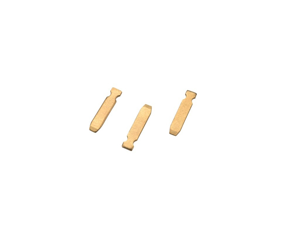
For prototype programs needing 50 to 500 pieces for design validation, or for low-volume production programs under 10,000 annual units, etching’s zero-tooling advantage makes it the only economically viable route.
This zero-tooling characteristic also makes etching the preferred platform for design iteration. A lead frame geometry undergoing three to five revisions before finalizing for volume production incurs $500 to $2,000 per phototool revision —one-twentieth the cost of modifying a hardened progressive die insert. For electrical stamping components in early-stage semiconductor packaging programs where the die pad configuration and lead count are still evolving, etching enables rapid design iteration that stamping’s tooling lead time cannot support —a common scenario when comparing lead frame manufacturing routes.
The four-slide and etch comparison further illustrates that etching’s flexibility extends to complex multi-plane geometries at low volume for stamped electrical contacts where geometry complexity would otherwise demand expensive cam-actuated progressive die stations.
Ultra-Fine Feature Resolution
Chemical etching resolves features down to 0.05 mm trace and space —finer than the 0.15 mm minimum slot width achievable with progressive die stamping. The limiting factor in stamping is punch buckling: a punch narrower than 0.15 mm lacks the column strength to withstand the shearing force required to pierce copper alloy strip, and it deflects or fractures under load. Etching has no mechanical cutting force.
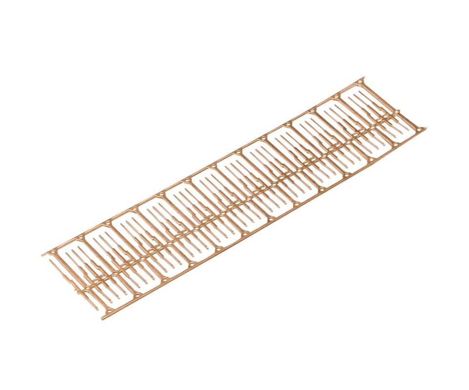
The etchant dissolves metal isotropically around the photoresist pattern, and feature resolution is limited only by photoresist adhesion and etchant undercut control.
This resolution advantage makes etching the dominant process for high-density lead frames where lead pitch drops below 0.40 mm and lead width falls below 0.15 mm. QFN and DFN packages with 0.35 mm lead pitch routinely use etched lead frames because stamping cannot reliably produce the required lead width and spacing. For bronze terminal stamping applications in standard-pitch connectors where lead width exceeds 0.20 mm, stamping’s resolution ceiling is not a binding constraint.
But for fine-pitch semiconductor packaging, etching is the only process that can deliver the required feature density.
Material Hardness Independence
Etching processes alloys that stamping cannot touch. High-strength copper alloys like C70250 Cu-Ni-Si at 400 HV, titanium alloys above 350 HV, and specialty alloys like Alloy 42 (Fe-42Ni) at 250 HV. These materials accelerate progressive die punch wear to unacceptable rates, requiring punch sharpening every 50,000 to 100,000 strokes instead of the 500,000-stroke interval standard for C19400 copper at 120 HV.
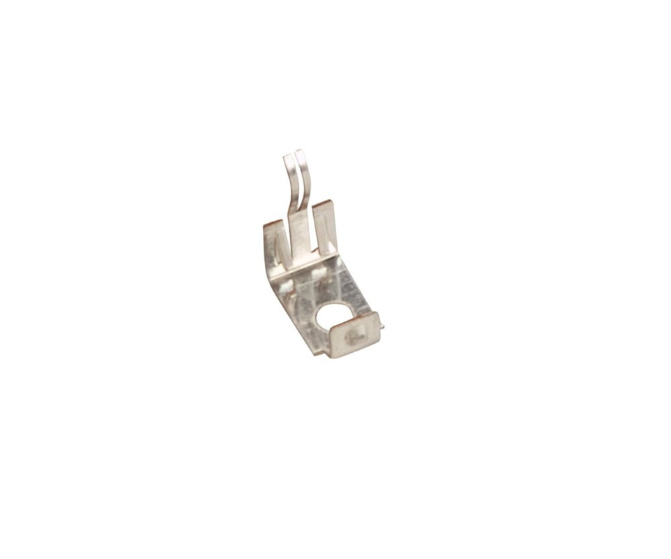
Chemical etchant attacks all these alloys at approximately the same rate regardless of hardness, because the etching mechanism is chemical dissolution, not mechanical shearing.
This hardness independence extends to material thickness as well. Stamping requires strip thick enough to maintain flatness during pilot-hole registration —0.08 mm minimum for copper alloys. Etching processes foil as thin as 0.025 mm without distortion because no mechanical force acts on the workpiece.
For semiconductor lead frames in ultra-thin packages where lead frame thickness below 0.10 mm is specified, etching is the only viable process. The combination of hardness tolerance and thin-foil capability makes etching essential for custom metal terminals in aerospace and medical applications where exotic alloy selection and ultra-thin profiles are dictated by application requirements rather than manufacturing convenience.
[Verdict]: If your lead frame requires sub-0.15 mm features, processes material harder than 300 HV, uses strip thinner than 0.08 mm, or has annual volume below 10,000 units, choose chemical etching.
Hidden Trade-offs & Engineering Limits
Edge Quality and Functional Impact
Stamped edges are sheared edges. They exhibit a characteristic profile of rollover, burnish, fracture, and burr zones. The burr height of 0.01 to 0.05 mm on a properly maintained progressive die is functionally acceptable for most terminal applications because the burr forms on the punch side of the strip and can be oriented away from the contact interface.
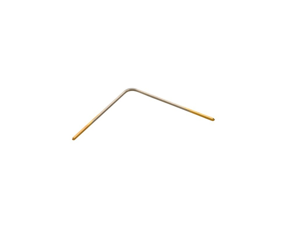
Etched edges are chemically smooth with no burr or mechanical deformation, but they exhibit a characteristic undercut. The etchant dissolves material laterally beneath the photoresist edge at approximately 15 to 25 percent of the material thickness. This undercut creates a trapezoidal cross-section rather than the vertical edge profile that a stamped part delivers.
For stamped electrical terminals where the terminal’s insertion edge slides against a connector housing ramp, the directionally controlled burr of a stamped part can actually reduce insertion force when oriented correctly —a phenomenon that etched parts with their smooth but trapezoidal edges cannot replicate. The burr direction control available in progressive die stamping is a functional design parameter, not just a quality variable, for terminals destined for low-insertion-force connector systems requiring sub-5 N engagement force.
Stress Relief and Grain Structure
Stamping cold-works the material along the sheared edge and formed bend radii —a beneficial effect for spring contacts where work hardening increases yield strength at the bend, improving contact normal force retention. The grain structure along the stamped edge is compressed and elongated in the direction of material flow, which improves fatigue resistance in cyclic loading applications. Etched parts undergo zero mechanical work.
The grain structure at the etched edge is identical to the bulk material, and the edge exhibits no work-hardening benefit.
However, this cold-work advantage comes with a stress concentration penalty. The stamped edge’s work-hardened zone is also a residual stress zone that can initiate stress corrosion cracking in environments with ammonia or sulfur compounds. Etched edges, free of residual stress, exhibit superior stress corrosion cracking resistance —a factor that matters for electrical stamping parts deployed in under-hood automotive environments where exposure to engine compartment chemicals accelerates stress corrosion in cold-worked copper alloys.
Part Design Freedom and Iteration Cost
Stamping imposes design constraints that etching does not. A progressive die requires a strip layout with carrier web, pilot holes, and a sequential station plan that determines the order of piercing, forming, and blanking operations. Changing any feature after the die is hardened means welding and re-cutting a die insert —a $2,000 to $8,000 modification that extends the tooling timeline by 1 to 3 weeks.
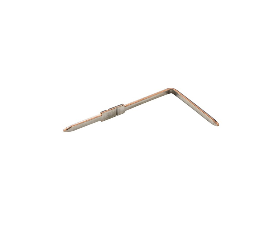
Chemical etching imposes no strip layout constraints —parts can be nested on a panel in any orientation, and a design change requires only a new $500 phototool produced from revised CAD data within 3 days.
This design freedom makes etching the preferred process for programs where the terminal geometry is not yet frozen. For electrical stamping manufacturers producing custom parts, guiding a customer through three design iterations with etched prototypes before committing to a $35,000 stamping die is standard practice —the $1,500 in cumulative phototool cost is negligible insurance against a $35,000 die that requires rework because the contact interface geometry changed between prototype approval and production kickoff. Kravzik offers both paths for stamped electrical terminals, using rapid etched prototypes to freeze the design before cutting steel for the production progressive die —a dual-path approach that eliminates the tooling rework risk for programs with evolving geometry requirements.
Critical Risk: Assuming stamping is always cheaper at high volume ignores the design iteration cost. A terminal program that undergoes three geometry revisions after die build accumulates $6,000 to $24,000 in die modification costs —more than the entire etched prototype program cost for 1,000 pieces. Always freeze the design with etched prototypes before commissioning a progressive die for stamped electrical terminal production.
💡 Process Selection Review: send us your lead frame or terminal drawing with annual volume and material specification for a dual-path stamped-versus-etched cost analysis with tooling, per-part economics, and lead time comparison.
The Final Call
Etching a fine-pitch terminal at production volume costs triple what stamping would deliver because the process was locked during prototyping. Kravzik evaluates your terminal against both paths with transparent cost data and an etched-prototype-to-stamped-production roadmap for programs that scale.
Send us your terminal drawing for a dual-path stamped-versus-etched cost analysis with tooling amortization, per-part economics, and a production roadmap, returned within 3 business days.