A burr height of 0.05 mm on a stamped electrical terminal transfers to the mating connector contact and raises contact resistance by 8—15 mΩ within 500 insertion cycles —a failure invisible on the dimensional inspection report but catastrophic for signal integrity.
In this guide, you will learn die clearance optimization by material temper, punch edge condition monitoring, burr measurement standards, and defect prevention for burr-induced failures.
Read on for the full DFM guide.
Die Clearance and Material Hardness Interaction
Burr height on stamped electrical terminals is not a byproduct of tool wear alone. It is a predictable function of the clearance between punch and die multiplied by the material’s resistance to fracture. When clearance widens beyond the recommended range, the strip material flows into the gap as a tensile tear rather than a clean shear, producing a raised ridge on the punch exit side.
This ridge height, measured from the terminal surface to the burr peak, directly determines whether the part passes dimensional inspection at the press line or generates a rejection batch flagged at the connector assembly station.
The Clearance-to-Burr Height Curve
Die clearance for stamped electrical terminals in C26000 brass must stay at 10—12% of material thickness per side to produce a burr height below 0.025 mm —the upper limit for IATF 16949 automotive-grade terminals. At 12% clearance on 0.64 mm strip (0.077 mm per side), the punch penetrates approximately 40% of the material thickness before fracture initiates, producing a burnish zone that occupies 35—40% of the sheared edge and a burr under 0.02 mm. At 18% clearance (0.115 mm per side), fracture initiates at 60—65% penetration and the burnish zone collapses to under 15%, leaving a burr that measures 0.05—0.08 mm from the characteristic tear-zone elongation at the punch-exit corner.
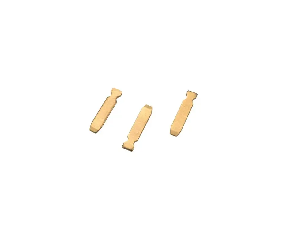
The clearance-to-burr curve is not linear across the 10—18% range. The slope steepens sharply above 15% clearance because the material transitions from a mixed shear-fracture mode to a dominant tensile-tear mode at that threshold. For production runs exceeding 500,000 strokes on a single die set, clearance must be monitored at every 50,000-stroke interval because punch-to-die alignment drift from press ram deflection adds 0.01—0.02 mm of effective clearance per 100,000 strokes.
[CAD Takeaway]: Specify a die clearance of 10—12% of material thickness per side in the tooling notes for C26000 brass terminals —this is a starting parameter the tooling team adjusts by ±1% based on the strip temper certificate from the mill.
Material Hardness Compensation Factors
Harder tempers reduce the fracture propagation window, requiring clearance to narrow or the burr penalty escalates rapidly. C17200 beryllium copper at full-hard temper (1,200 MPa tensile strength) demands 8—10% clearance per side instead of 10—12% —the higher yield strength delays fracture initiation until the punch has penetrated 30—40% deeper into the strip cross section. At 12% clearance, C17200 produces burrs 2× higher than the same clearance on C26000 because the material resists shear localization and instead extrudes into the die gap as a continuous raised ridge.
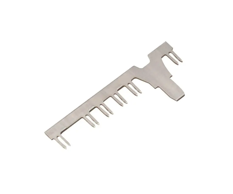
The comparison data above summarizes clearance compensation factors across common copper alloys used in terminal stamping.
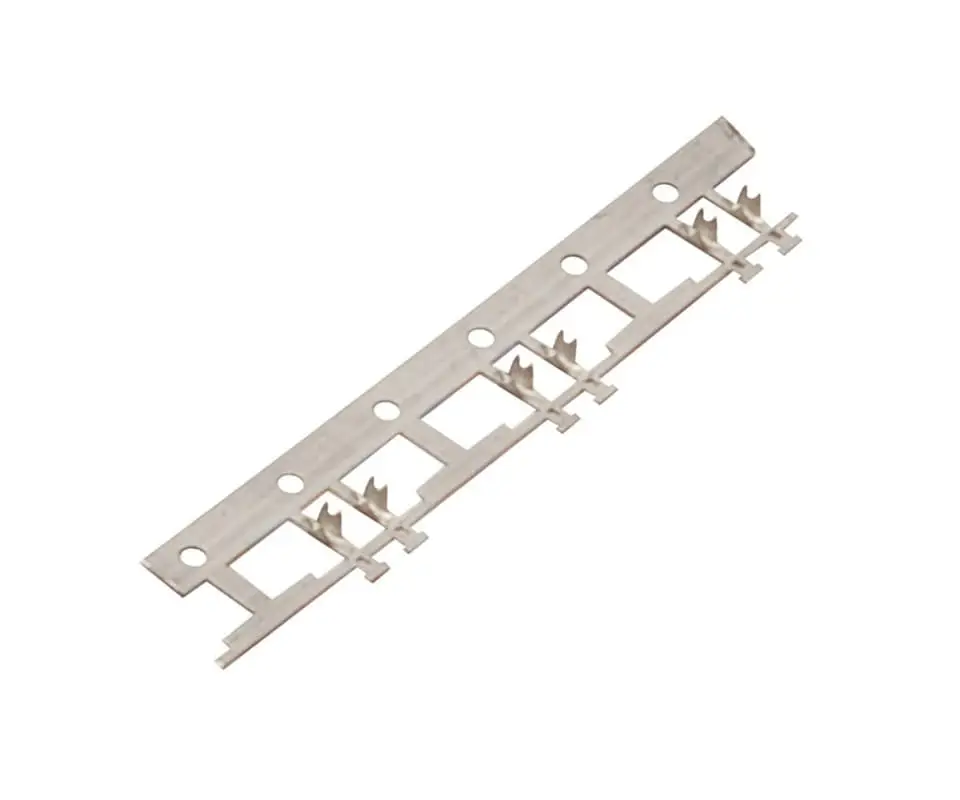
The inverse relationship holds for softer alloys. C11000 electrolytic tough pitch copper at annealed temper tolerates clearance up to 14—15% per side while maintaining burr height below 0.025 mm. The lower yield strength (70 MPa annealed vs.
250 MPa half-hard C26000) allows shear localization to dominate across a wider clearance window. For mixed-material progressive dies running multiple copper alloys on the same strip, Kravzik selects a single clearance value at the midpoint range that keeps all materials below 0.025 mm burr —typically 11% for a C26000/C11000 combination die.
[CAD Takeaway]: Note the terminal material temper on the drawing (e.g., “C17200 FH” or “C26000 HH”) —the tooling team adjusts clearance by ±2% from the baseline based on this temper designation.
Punch and Die Edge Condition
The clearance number on the tooling drawing is useless if the cutting edges carry a radius larger than the specified clearance itself. Punch edge radius growth from adhesive wear on copper alloys is the single largest variable in burr height production-line data. It changes the effective shearing mechanism from cutting to extrusion without any change in the nominal die clearance setting on the press.
Edge Radius vs Effective Cutting Mode
A new D2 tool steel punch carries a cutting edge radius of approximately 0.005—0.010 mm after final grinding. At 50,000 strokes on C26000 brass, adhesive wear from copper transfer to the punch face raises this radius to 0.015—0.020 mm —still within the shearing regime where the material fractures cleanly at the penetration depth predicted by the clearance ratio. The problem emerges between 80,000 and 120,000 strokes, when the edge radius exceeds 0.025 mm and the cutting mechanism shifts from shear-initiated fracture to compressive extrusion.
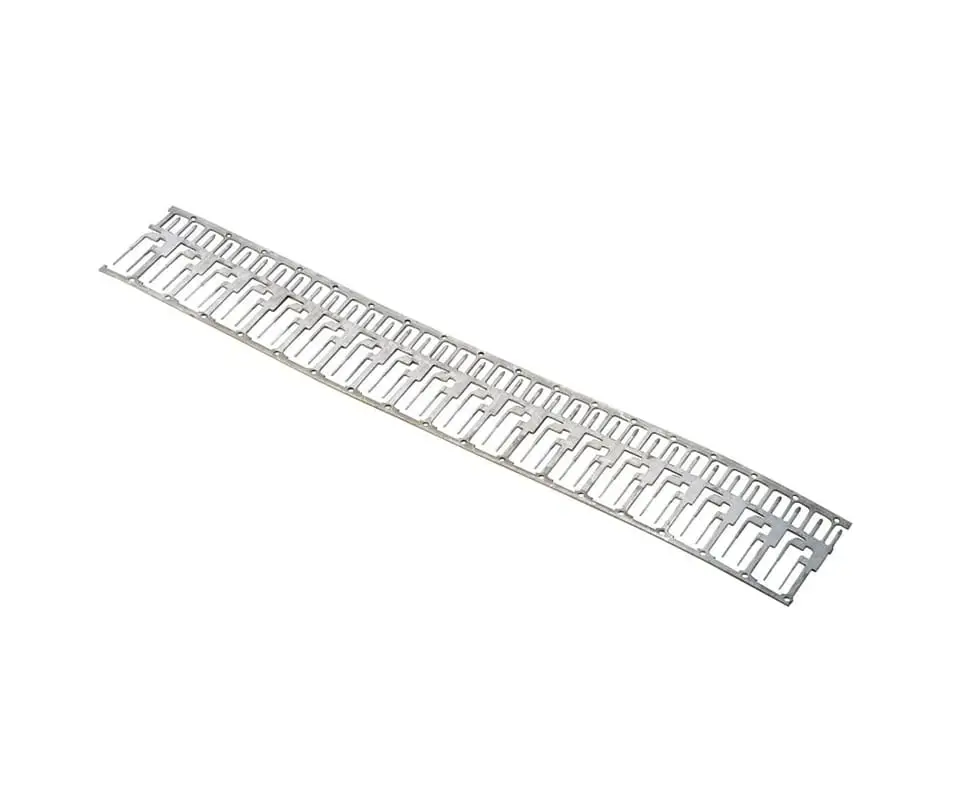
The table above maps punch edge radius growth to the resulting burr height across the progressive die lifecycle.
At an edge radius above 0.025 mm, the punch no longer initiates a fracture at the strip surface. Instead it compresses the material into the die cavity before the shear stress reaches the fracture threshold. The resulting burr doubles in height from 0.02 mm to 0.04 mm in a single measurement interval —typically 5,000 strokes —because extrusion produces a continuous raised ridge around the entire punched profile rather than the localized tear peaks characteristic of correct shear-mode cutting.
For high-speed progressive die tooling running at 400—600 SPM, this transition happens within 30—40 minutes of continuous operation.
[CAD Takeaway]: Include a punch edge inspection interval in the tooling maintenance schedule —every 50,000 strokes for C17200 beryllium copper and every 80,000 strokes for C26000 brass, with immediate regrind at 0.025 mm edge radius or above.
Die Wear and Clearance Drift Compensation
Die wear on the exit side produces an asymmetric clearance condition that generates burrs on only one edge of the terminal profile —a signature that helps maintenance teams distinguish die-wear burrs from punch-wear burrs. When the die bore diameter increases by 0.01 mm from abrasive wear, the clearance on the punch exit side increases by an equivalent amount while the opposite side remains at the original setting. This asymmetric condition produces a burr height difference of 0.015—0.025 mm between the two edges, detectable within a single CMM measurement cycle.
The table above maps die bore diameter increase to the resulting clearance asymmetry and burr height bias.
Compensation requires a dynamic clearance adjustment on the press, not just a die regrind. Kravzik‘s progressive dies for custom metal terminals incorporate a shim-adjusted die shoe that allows the die half to be repositioned by 0.005—0.010 mm increments without removing the tool from the press. When burr height measurements show a 0.02 mm bias toward one edge, the die half is shimmed to restore symmetric clearance, recovering burr conformity within one adjustment cycle without the downtime of a full die pull.
[CAD Takeaway]: Design the die set with shim-adjustable die shoe positioning that allows 0.005 mm incremental clearance correction —this single feature eliminates the need for a full die pull when asymmetric burr formation appears mid-run.
💡 Clearance Audit: verify die clearance against temper certs and return a burr height Cpk projection before tool steel is cut.
Burr Measurement Standards and Tolerancing
A burr height specification without a defined measurement protocol is not a quality requirement. It is a wish. The measurement method, sampling position, and acceptance criteria must be explicit on the terminal drawing for the specification to be enforceable at both the press line and the customer’s incoming inspection station.
Measurement Methods and Sampling Positions
Three measurement methods appear on terminal drawings, and they produce different readings from the same part. Optical profilometry scans the edge profile at 200× magnification and captures the burr peak to a resolution of 0.001 mm, making it the reference method for electrical stamping components where a 0.005 mm burr height variation shifts contact resistance. Digital micrometer measurement at the edge captures the combined burr-plus-material thickness, overstating the burr by 0.005—0.010 mm because the anvil contacts the burr peak while the spindle contacts the opposite surface.
Visual comparison against a burr standard chart (ASTM B850) provides rapid go/no-go sorting at 30× magnification but misses burrs under 0.015 mm that a profilometer would register.
Sampling position matters as much as the method. Burr height must be measured at three positions per terminal edge —the edge center and 2 mm from both ends —to detect the localized clearance variation from uneven punch-to-die alignment. A center-only measurement misses end-position burrs that contact the connector housing first during insertion.
For multi-cavity progressive dies, every cavity must be sampled independently because punch-to-die clearance varies by 0.005—0.010 mm across a 4-cavity die set due to thermal expansion differences between the punch holder and die block.
[CAD Takeaway]: Specify “Burr height per optical profilometry at 200×, three positions per edge (center, left 2 mm, right 2 mm), max 0.025 mm” in the terminal drawing notes.
Industry Standard Burr Height Tolerances
IATF 16949 for automotive terminals defines burr height not as a single number but as a function of the terminal’s functional criticality. Class A terminals —those carrying signal current through a separable contact interface —require burr height below 0.025 mm on all functional edges. Class B terminals for power distribution allow burr height up to 0.05 mm because the higher normal force (5—15 N vs.
0.5—3 N for signal contacts) mechanically crushes the burr during the first insertion cycle, effectively self-correcting the defect. ASTM B850 provides the visual comparison reference standard but does not define acceptance limits —those must come from the customer specification or the IATF class designation.
The gap between the 0.025 mm IATF Class A limit and what a well-maintained progressive die can actually produce (0.010—0.015 mm) represents the process capability margin. When Cpk drops below 1.33 —meaning the burr height distribution has shifted so that the upper tail touches 0.025 mm —corrective action is required even though no individual part has exceeded the specification. Kravzik monitors burr height Cpk at every 25,000 strokes through automated optical profilometry integrated into the press line, flagging the trend before a single nonconforming terminal leaves the die.
[CAD Takeaway]: Designate the terminal’s IATF class (A, B, or C) on the drawing and reference the specific burr height limit associated with that class —this tells the tooling team the acceptable Cpk floor.
Defect Prevention —Burr-Induced Failure Modes
A burr that passes dimensional inspection can still cause a field failure if it locates on a functionally sensitive surface. Two failure modes dominate burr-related warranty returns for stamped electrical terminals: contact resistance drift from burr material transfer and plating void formation at the burr root.
Burr Transfer and Contact Resistance Drift
When a terminal with a 0.04 mm burr on the contact beam undergoes repeated insertion cycles, the burr acts as a micro-abrasive against the mating connector surface. Each cycle scrapes a sub-micron layer of terminal material —typically tin or silver plating —onto the mating contact, building an oxide layer that raises contact resistance by 8—15 mΩ within 500 cycles. At 1,000+ cycles, the contact resistance exceeds the 20 mΩ threshold that triggers a signal integrity failure in automotive sensor circuits, where low-current signals (5—50 mA) cannot penetrate the oxide film that the transferred burr material has deposited on the mating surface.
The table above catalogs how burr transfer accumulates across insertion cycles and drives contact resistance upward.
The failure is invisible to single-cycle dimensional inspection because the burr height meets the 0.025 mm spec —but the burr’s position on the contact beam rather than a non-functional edge makes it a functional defect. Prevention requires separating the burr location specification from the burr height specification on the terminal drawing: “Burr height ≥0.025 mm on all edges. Burr on the contact beam surface ≥0.015 mm regardless of the general tolerance.” This distinction eliminates the false confidence that a passing dimensional report provides when the burr is positioned on a wear-sensitive surface.
[CAD Takeaway]: Add a separate burr height tolerance for contact surfaces and wear surfaces on the terminal drawing —differentiate them from the general edge burr tolerance to prevent burr-induced contact resistance drift.
Plating Void Formation at the Burr Root
The burr root —the transition zone where the burr meets the terminal surface —creates a geometric discontinuity that disrupts electroplating current density distribution. The sharp angle at the burr root concentrates current density during plating, causing a locally thinner deposit at the burr base that measures 50—70% of the nominal plating thickness. When the terminal is later subjected to thermal cycling (common in engine-bay connectors cycling from −?strong>40°C to 125°C), the thin plating at the burr root cracks first, exposing the base copper alloy to fretting corrosion that generates non-conductive copper oxide within 200—00 thermal cycles.
The comparison data above quantifies the plating thickness deficit at burr root locations across standard electroplating processes.
Deburring alone does not solve the plating problem —it removes the burr peak but leaves the burr root geometry that still concentrates plating current. The DFM solution is to specify a minimum edge break radius of 0.05—0.08 mm after deburring on all edges that will receive electroplated tin or precious metal coating. This radius creates a smooth transition that allows uniform current distribution across the edge during the plating bath, restoring plating thickness to ≥strong>90% of the nominal value at the former burr location.
[CAD Takeaway]: Call out a minimum 0.05 mm edge break radius after deburring on all plated edges —this prevents the burr root from concentrating plating current and creating a thin-spot that cracks during thermal cycling.
💡 Burr Root Cause Analysis: send your terminal drawing for burr DFM covering clearance optimization, edge condition thresholds, and plating compatibility —delivered within 48 hours.
CAD to Production
Generic die clearance values applied without temper certificate verification produce burr heights that pass visual inspection but fail Cpk at incoming QC. Kravzik’s tooling engineers verify clearance against actual material certs before steel is cut and return a written DFM analysis within 48 hours.
Send us your terminal print for a burr height DFM review covering die clearance, edge condition, and plating compatibility, delivered within 48 hours under NDA protection.