A compliant pin with a 0.02 mm interference error in its press-fit zone produces 300 N insertion force against a 150 N spec — bowing the PCB, cracking the barrel plating, and scrapping a $12 multi-layer backplane before it reaches functional test. When the beam geometry is wrong by 20 microns, the claim hits the warranty desk, not the test bench.
In this guide, you will learn compliant zone geometry design rules, interference fit tolerance stack calculation, insertion and retention force limits, and the stamping-specific parameters that produce press-fit stamped electrical terminals with gas-tight connections across the full PCB manufacturing tolerance range.
Read on for the full DFM guide.
Fundamental Geometry & Compliant Zone Design
Compliant Zone Geometry Parameters
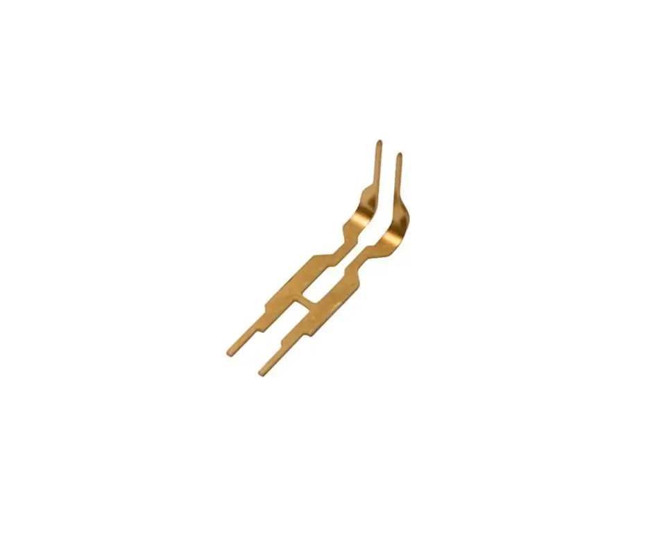
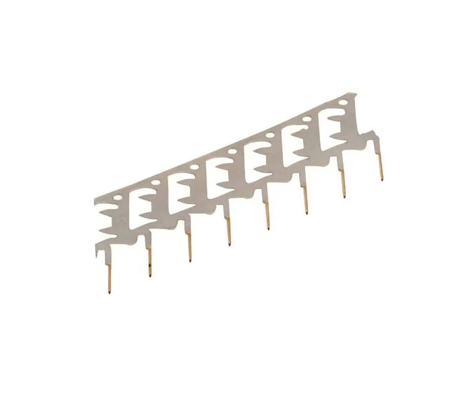
A compliant pin — also called an eye-of-needle (EON) or press-fit pin — replaces soldering with mechanical interference. The pin’s compliant section, typically an eye-shaped opening with two or four spring beams, compresses radially during insertion into a plated through-hole (PTH) and exerts continuous normal force against the hole wall. This normal force creates a gas-tight electrical connection that maintains contact resistance below 1 mΩ across the product’s service life without the solder joint that dominates traditional through-hole assembly.
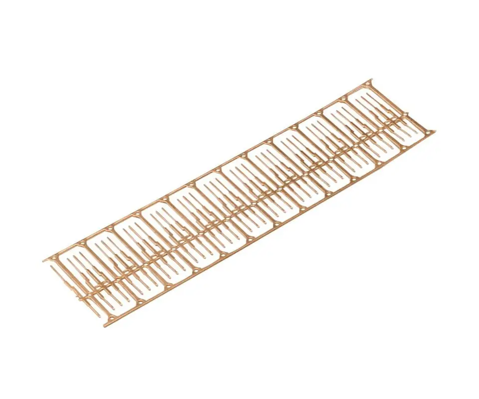
The compliant zone geometry is defined by four critical dimensions: the beam width, the beam length, the eye opening width, and the overall press-fit zone width. The beam width — typically 0.20 to 0.40 mm for stamped copper alloy terminals — dictates the spring rate. A wider beam produces higher insertion force and higher retention force.
The beam length — typically 0.80 to 2.00 mm — determines the elastic deflection range. A longer beam can accommodate larger hole tolerance variation without yielding. The eye opening — the distance between the two beams at the widest point — controls the interference range.
A larger eye opening requires more compression to contact the hole wall, shifting the force curve to higher interference values for stamped electrical connectors in press-fit applications.
Press-Fit Zone Width & Interference Calculation
One of the most critical dimensions is the overall press-fit zone width — the distance from beam tip to beam tip before insertion — and this dimension alone determines whether the pin survives or yields. The press-fit zone width must exceed the maximum PTH finished hole diameter by 0.03 to 0.08 mm, ensuring interference across the full tolerance range. A pin designed for a 1.00 mm ±0.05 mm PTH requires a press-fit zone width of approximately 1.08 to 1.13 mm — producing 0.03 mm of interference at the maximum hole (1.05 mm) and 0.08 mm at the minimum hole (0.95 mm).
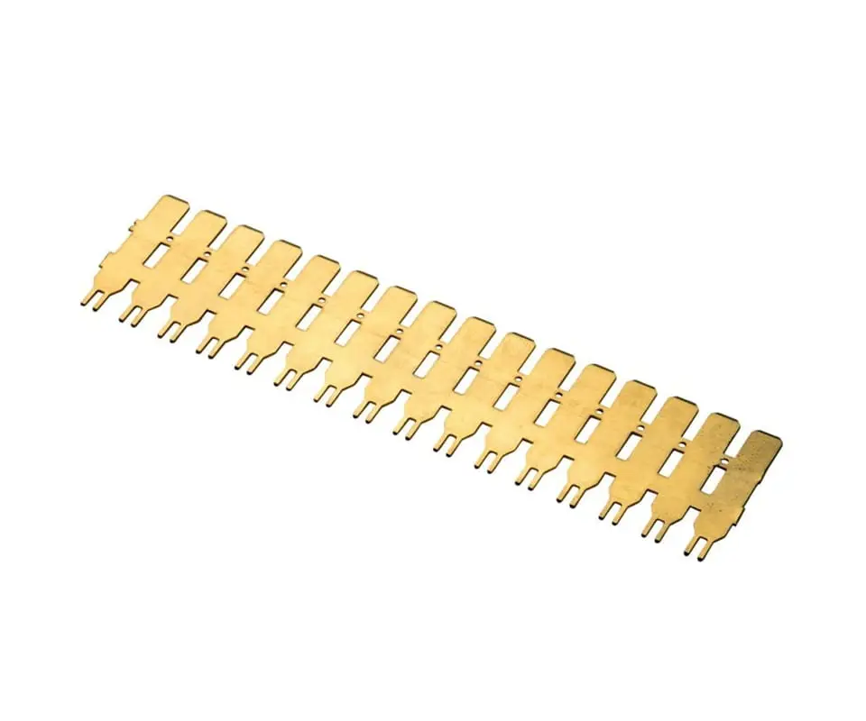
At 0.08 mm of interference, the beam stress must remain below 80 percent of the alloy’s yield strength to prevent permanent deformation.
[CAD Takeaway]: Design the compliant pin press-fit zone width to produce 0.03–0.08 mm of diametral interference across the full PCB hole tolerance range, and verify through FEA simulation that beam stress at maximum interference stays below 80 percent of yield strength for the specified stamped terminal alloy.
Tool-Specific Constraints & Progressive Die Integration
Pierce-and-Coin Process Design
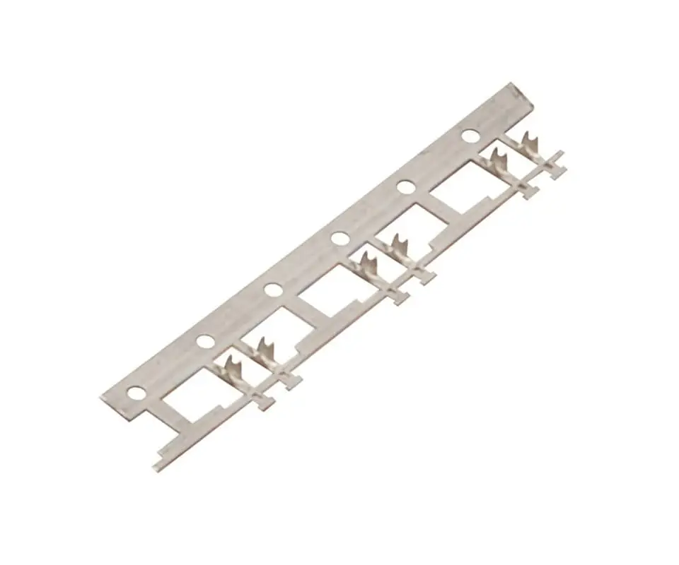
Stamping a compliant pin requires the progressive die to pierce the eye opening, profile the beam contours, and form the pin to final thickness — all while maintaining the beam width tolerance that controls the spring rate. The eye opening is typically pierced at 60 to 80 percent of the material thickness in the first piercing station, then coined to final width in a subsequent station that compresses and work-hardens the beam tips. This two-step process — pierce then coin — produces a beam with controlled work hardening at the tip that improves elastic recovery after compression.
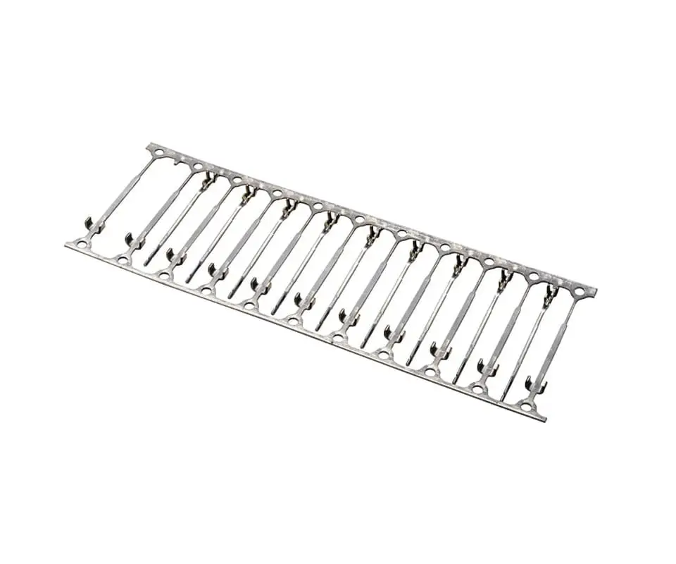
The coining station is the most critical tooling element in the compliant pin die. It must reduce the beam tip thickness by 10 to 20 percent — from the nominal strip thickness of 0.64 mm down to approximately 0.55 mm at the beam tip — while maintaining the beam width within ±0.01 mm. A coining reduction below 10 percent does not stabilize the grain structure at the beam tip and the pin takes a permanent set during insertion.
A reduction above 25 percent thins the beam excessively and reduces the retention force below the 20 N minimum. Kravzik‘s progressive die tooling for compliant pin stamped electrical terminals includes a dedicated coining station with an automatic thickness feedback loop that adjusts the coining stroke based on incoming strip thickness measured at the first station.
Coining Station Control & Alloy Selection
Material selection for compliant pins is dominated by two alloys. C70250 Cu-Ni-Si offers high yield strength (650–750 MPa after stamping and aging) with 40 to 50 percent IACS conductivity — the optimal balance of spring force and current-carrying capacity for power press-fit applications. C51000 phosphor bronze offers moderate yield strength (480–550 MPa) with 15 percent IACS conductivity — sufficient for signal-level press-fit pins in high-density connectors where current per pin is below 3 A.
[CAD Takeaway]: Specify a two-step pierce-and-coin process for the compliant pin eye opening in the progressive die strip layout, with the coining station reducing beam tip thickness by 15 percent of nominal to stabilize grain structure and ensure elastic recovery after insertion.
The alloy selection also drives the coining force requirement and the corresponding press tonnage. C70250 at 650 MPa yield in the annealed condition requires approximately 20 percent more coining force than C51000 at equivalent strip thickness, which means the coining station must be designed with carbide inserts and a reinforced punch holder to resist deflection under load. A coining punch that deflects by even 0.005 mm under load produces a beam thickness gradient across the eye opening — the beam tip closest to the punch center thins more than the opposite tip — and this asymmetry creates an insertion force imbalance that rotates the pin during press-fit and scores the PCB hole barrel.
Precision, Tolerancing & Force Verification
Insertion Force Limits & Verification
The insertion force window for a compliant pin is bounded by two constraints. The upper bound is the maximum force the PCB can absorb without bowing — typically 60 N per pin for a 1.6 mm thick FR4 board at room temperature. The lower bound is the minimum force required to retain the pin against vibration and thermal cycling — typically 20 N per pin per IEC 60352-5 for press-fit connectors.
The stamped pin must operate between these two limits across the full PCB hole tolerance range, the full pin dimensional tolerance range, and the full temperature range of the application.
Insertion force verification uses a force-versus-displacement curve captured during pin insertion into a calibrated test coupon. The insertion force rises as the pin enters the hole, peaks at the widest point of the press-fit zone, and then drops to a residual sliding force as the pin body passes through the hole. The peak insertion force must fall between 30 and 55 N — below the 60 N PCB damage threshold but with margin above the 20 N retention minimum.
Retention Force & Thermal Cycle Validation
Kravzik‘s press-fit validation protocol for stamped electrical terminal compliant pins captures the force curve on 30 consecutive insertions at the start, middle, and end of a production run to establish process capability for insertion force within the specified window.
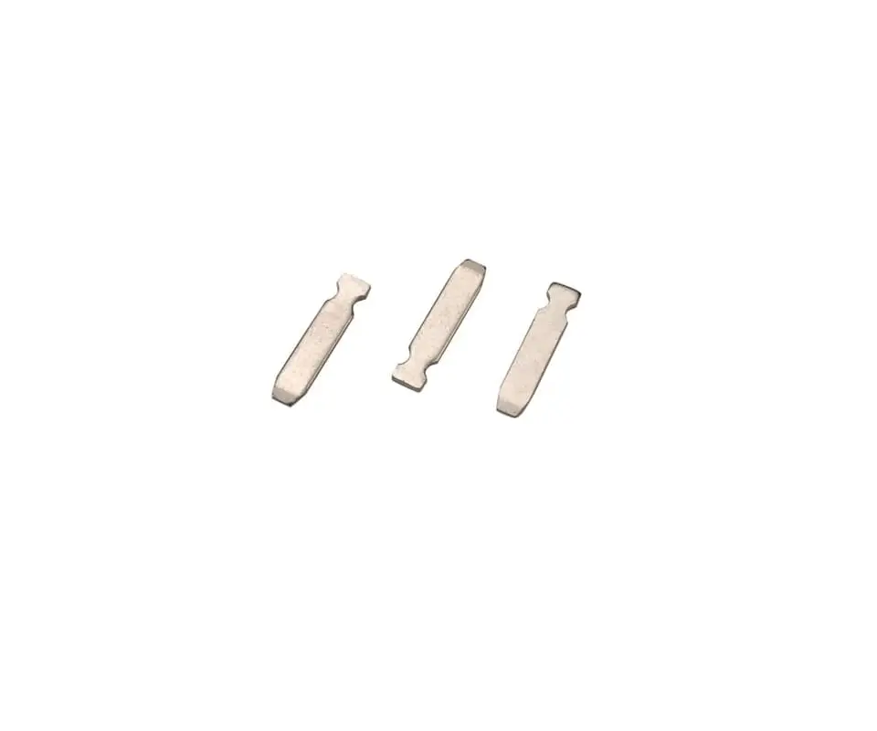
Retention force is measured by pulling the pin out of the test coupon at 25 mm per minute and recording the peak force. The retention force must exceed 20 N per IEC 60352-5, and should show less than 10 percent degradation after 500 thermal cycles from -40 degrees C to +105 degrees C — simulating the solder-reflow and thermal cycling profile that a press-fit connector experiences in automotive ECU and power distribution applications.
[CAD Takeaway]: Verify compliant pin insertion force at 30 to 55 N peak and retention force above 20 N per IEC 60352-5, with less than 10 percent retention force degradation after 500 thermal cycles from –40°C to +105°C, validated on actual PCB test coupons with the specified hole diameter and plating finish.
Defect Avoidance & Failure Mode Prevention
Beam Yield & Hole Barrel Damage
The three most common failure modes for stamped compliant pins are beam yield, hole barrel damage, and whisker growth. Beam yield occurs when the interference fit exceeds the alloy’s elastic limit. The beams compress plastically and lose normal force, resulting in intermittent contact after thermal cycling. Prevention requires FEA simulation of the beam stress at maximum interference and verification that stress stays below the alloy’s 0.2 percent offset yield strength with a safety factor of 1.25.
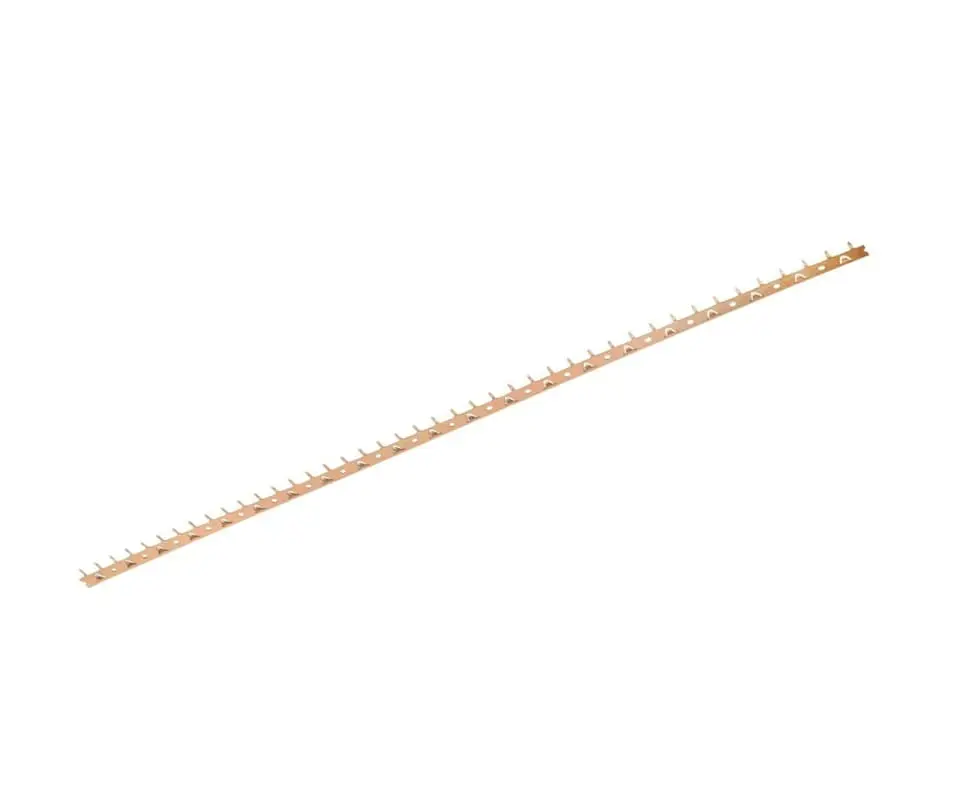
Hole barrel damage occurs when the pin tip geometry is too sharp or when the insertion is misaligned by more than 2 degrees from the hole axis. The pin tip scrapes the copper barrel instead of centering in the hole, reducing the barrel wall thickness and potentially exposing the FR4 substrate. Prevention requires a chamfered or radiused pin tip with a lead-in angle of 20 to 30 degrees and an insertion fixture that constrains alignment to within 1 degree of perpendicular to the PCB surface for electrical stamping parts in press-fit connector assembly.
Tin Whisker Mitigation Strategy
Tin whisker growth from the press-fit zone is a risk for pure tin-plated pins in high-density connectors where the pin-to-pin spacing is below 0.50 mm. The compressive stress in the press-fit zone can drive whisker nucleation at the tin grain boundaries.
Mitigation follows JESD201. A 1.5 to 2.0 µm nickel underplate between the copper alloy substrate and the tin top layer blocks copper-tin intermetallic formation, and a 150 degrees C post-plating anneal within 24 hours of plating relieves residual plating stress.
[CAD Takeaway]: Apply a nickel underplate of 1.5–2.0 µm between the copper alloy substrate and tin top layer for compliant pins, and specify a 150°C post-plating anneal within 24 hours per JESD201 to mitigate tin whisker growth risk from press-fit zone compressive stress.
The press-fit zone geometry itself amplifies whisker risk because the compressive hoop stress after insertion into the PCB hole adds to the residual plating stress, creating a combined stress state that accelerates nucleation. Finite element analysis of the post-insertion stress distribution shows that the beam tips experience the highest compressive stress concentration, and these are precisely the regions where whiskers nucleate first. For compliant pins in connectors with pin spacing below 0.40 mm, Kravzik recommends gold flash over the nickel underplate on the press-fit zone as a definitive whisker elimination strategy rather than relying solely on the post-plating anneal for mitigation.
CAD to Production
Compliant pin yielding during insertion traces back to beam width drifting per coil lot while the coining station stays set to the first coil. Kravzik’s die design includes FEA beam stress simulation and automatic coining adjustment based on incoming strip thickness, validated with 30-pin insertion force studies before shipment.
Request a press-fit die design with FEA-validated beam stress analysis and IEC 60352-5 compliance verification, returned within 3 business days.