A terminal drawing passes the dimensional layout review at nominal condition. Four months into production, the connector qualification test fails at thermal cycle 800 as contact resistance crosses the 10 mΩ reject threshold. The dimensional print was correct. The 4 of 7 design parameters that govern in-service reliability were never checked at IQC.
In this guide, you will discover the 7 design parameters that determine whether a stamped electrical terminal survives connector qualification – alloy selection rule, bend radius minimum, contact normal force derating, plating thickness profile, retention lance geometry, insertion chamfer design, and tolerance stack strategy.
Read the breakdown.
Alloy Selection
Key Advantage
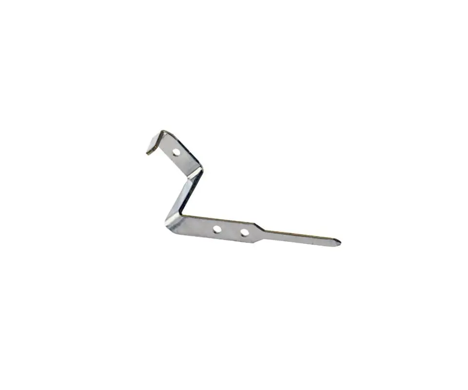
The alloy grade determines the contact normal force ceiling and the stress relaxation rate. C17200 beryllium copper retains 95% contact force at 150°C after 1000h. C11000 copper retains 80% at 100°C.
The selection decision upstream of the die design controls the downstream failure rate in high-temperature stamped terminal production.
Best Used For
Map alloys to applications: C11000 for single-use or low-cycle power terminals below 80°C; C51000 for signal terminals with 5,000–10,000 cycles below 125°C; C17200 for high-cycle or high-temperature terminals above 125°C. The following table compares the thermal performance of common terminal alloys.
| Alloy | Temp Ceiling | Force Retention | Mating Cycles | Typical Application |
|---|---|---|---|---|
| C11000 | 80°C | Low | < 50 | Busbars / Power lugs |
| C51000 | 125°C | Medium | 5,000 | Automotive sensors |
| C17200 | 150°C | High | > 10,000 | Battery connectors |
The Trade-off
Higher strength alloys like C17200 cost 4–6x more than C11000 on a per-kilogram basis and require 8–12 week mill lead time with beryllium safety compliance. The over-spec penalty is material cost. The under-spec penalty is field failure caused by excessive stress relaxation.
Bend Radius
Key Advantage
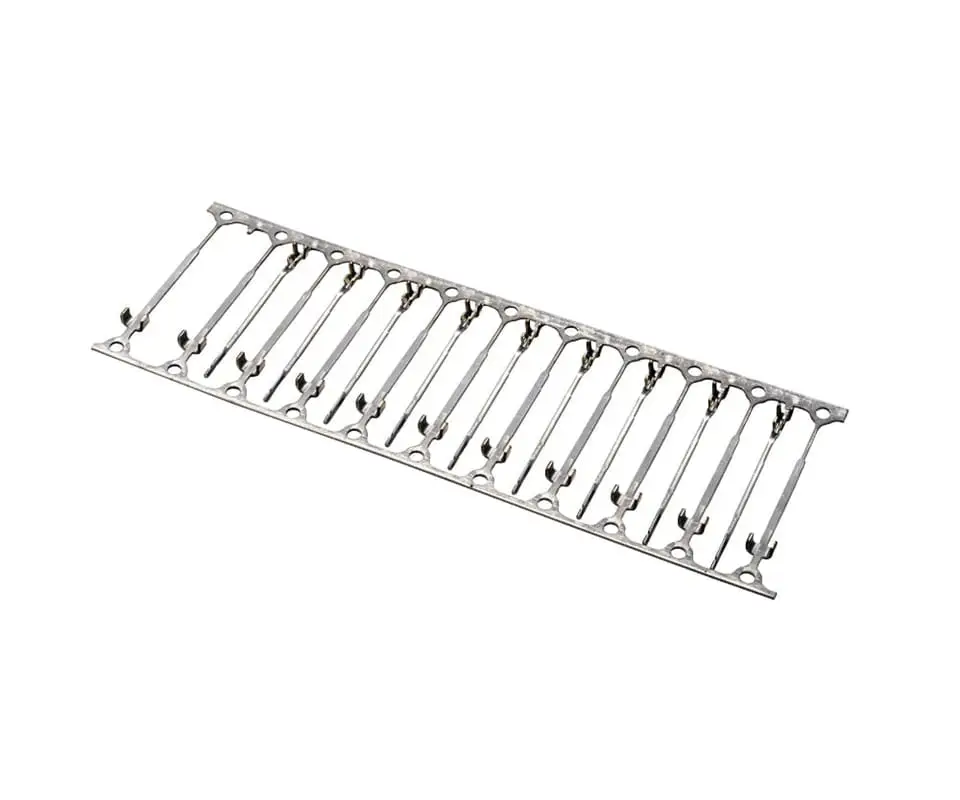
Minimum bend radius controls whether the terminal can be stamped in one progressive die or requires a secondary forming station. C11000 allows 0.5t minimum bend radius.
C17200 age-hardened requires 3.0t. Every terminal with bends below 1.5t must use C11000, C19400, or C17200 in the solution-treated (AT) condition before age hardening.
Best Used For
Terminals with multi-bend geometries like contact beams and spring loops benefit from alloys with n-value above 0.20 – C11000 (0.35), C19400 (0.22). Terminals with single-bend geometries such as simple blade contacts can use lower-n alloys with higher strength to minimize tool wear in the progressive die tooling.
The Trade-off
Designing below the minimum bend radius causes micro-cracks at the bend apex that reduce fatigue life by 3–5x regardless of alloy fatigue limit. The “tight bend, smaller connector” goal collides with the “no micro-crack” requirement at approximately 1.0t for C19400 and 1.5t for Brass 260.
Contact Normal Force
Key Advantage
Contact normal force must exceed 2.0N at maximum operating temperature (including stress relaxation derating) to penetrate the tin oxide layer at the contact interface. A terminal measuring 3.5N at 23°C IQC may deliver only 2.1N at 105°C after 1000h – a 40% derating that crosses below the threshold.
Best Used For
Any tin-plated terminal in a sealed engine-bay connector with ambient temperature above 80°C requires contact force validation at 1000h thermal aging. The 2.0N threshold per IEC 60512-2 is the engineering minimum – the design should target 3.0N at 23°C to maintain 2.0N after derating.
The Trade-off
Higher contact normal force requires a stiffer contact beam, which increases insertion force and mating cycle wear. Every 0.5N increase in contact force above 3.0N adds approximately 1.5N to the insertion force per contact, which becomes material for a 64-pin connector.
Plating Thickness Profile
Key Advantage
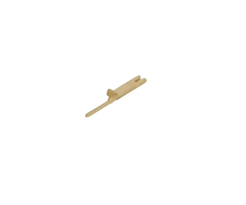
Tin plating thickness must be measured at the contact beam bend apex – not on the flat shank. Electroplating current density inside the bend radius is lower, producing 30–50% thinner plating at the exact point where contact is made and oxide film penetration is required. This requires a supplier with a high-performance in-house plating line.
Best Used For
Minimum 2.5 µm tin plating at the bend apex per ASTM B545 is required for terminals in environments above 60% RH. For terminals with bend radii below 1.5t, a nickel strike layer of 1.0–2.0 µm is required before tin plating for C17200 and C51000 substrates.
The Trade-off
Thicker plating improves porosity performance but increases the risk of tin whisker formation. JESD201-compliant matte tin at 2.5–5.0 µm with 150°C/1hr post-plating anneal provides the optimal balance between corrosion resistance and whisker mitigation.
Retention Lance Geometry
Key Advantage
The retention lance engagement depth must be designed at 0.25–0.35 mm with Cpk over 1.33. A 0.10 mm engagement depth deviation reduces retention force from 80N to below 40N – causing terminal backout during harness assembly or vehicle operation.
Best Used For
All terminals in multi-pin connectors with vibration exposure (engine bay, chassis-mounted, door harness) require retention lance design with a die wear safety margin of 0.05 mm beyond the engagement minimum to ensure long-term reliability.
The Trade-off
Deeper lance engagement requires more material in the terminal body and a larger housing cavity, conflicting with connector miniaturization trends. Each 0.05 mm increase in engagement depth adds approximately 0.2 mm to the connector pitch.
Insertion Chamfer
Key Advantage
A terminal with a 30-degree insertion chamfer reduces peak insertion force by 25–40% versus a square-cut tip, decreasing harness assembly operator fatigue and reducing the risk of terminal buckling during automated insertion.
Best Used For
Terminals with wire gauge above 20 AWG or insertion into high-pin-count connectors (above 40 positions) benefit most from chamfered tips. The chamfer also guides the terminal into the housing cavity, reducing misalignment during blind-mate assembly.
The Trade-off
Chamfered tips reduce the available contact surface area on the tip, limiting current-carrying capacity at the leading edge. For power terminals above 15 A, the tip must remain flat to maximize contact area and prevent localized heating.
Tolerance Stack Strategy
Key Advantage
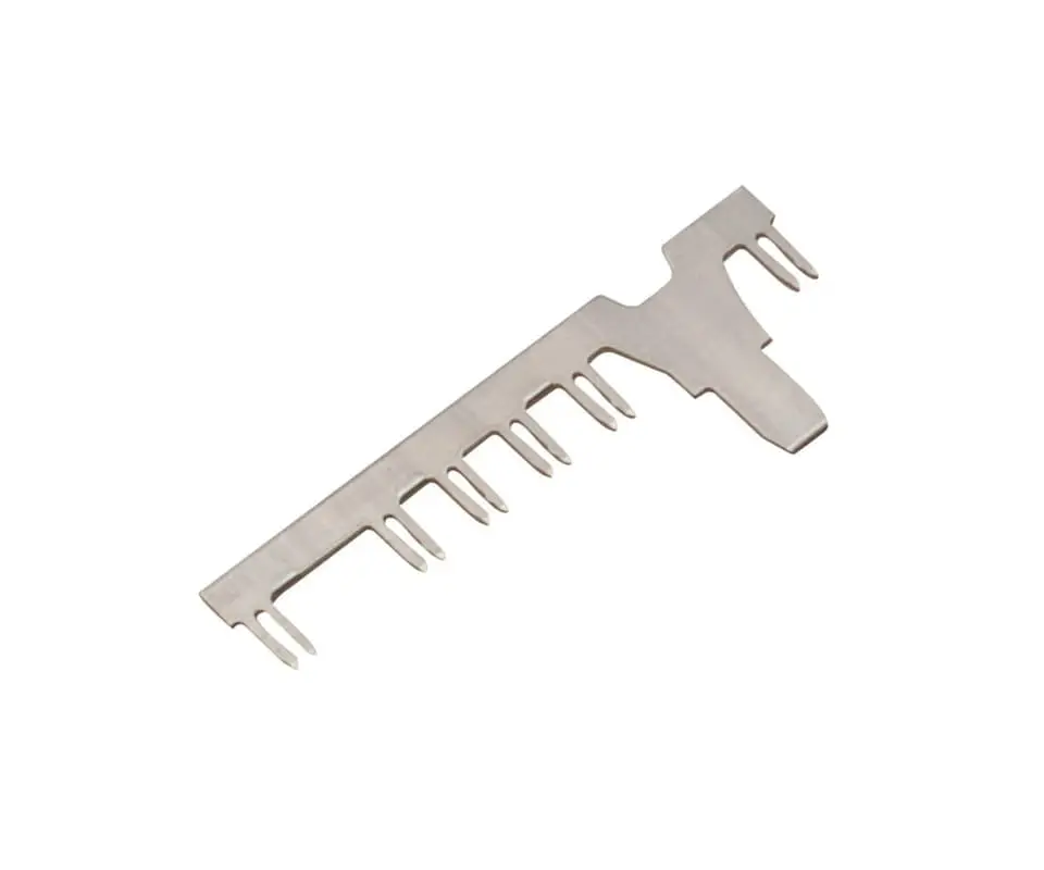
The tolerance stack across terminal width, housing cavity width, and retention feature position determines the assembled terminal’s lateral clearance – which directly controls fretting amplitude under vibration. A stack yielding 150 µm clearance places the terminal in the critical 25–75 µm fretting window. This must be managed within the quality management system.
Best Used For
Tolerance stack analysis must be performed in the design phase using worst-case or RSS (root sum square) methodology. The target: assembled lateral clearance below 100 µm for vibration-exposed terminals per USCAR-2.
The Trade-off
Tighter tolerances increase stamping and molding tooling cost by 15–30% for each 0.01 mm of additional precision. The stack must be loosened where possible (housing cavity) and tightened where essential (terminal width, lance position).
Design Parameters Summary
| Design Parameter | Design Target | Measurement Method | Accept Criterion | Consequences of Violation |
|---|---|---|---|---|
| Alloy Grade | T_max matching | Mill certification | ASTM B194 / B103 | Stress relaxation failure |
| Bend Radius | > 1.5t (Brass) | Optical comparator | No micro-cracks at 50x | Fatigue fracture |
| Normal Force | > 2.0N (derated) | Force-displacement test | IEC 60512-2 | High contact resistance |
| Plating Profile | > 2.5 µm (apex) | XRF on bend radius | ASTM B545 | Porosity & corrosion |
| Lance Depth | 0.25–0.35 mm | Vision inspection | Cpk > 1.33 | Terminal backout |
| Insertion Chamfer | 30° angle | Shadowgraph | ± 5° tolerance | Buckling & high insertion force |
| Lateral Clearance | < 100 µm | RSS Tolerance Stack | USCAR-2 | Fretting corrosion |
Your Quick Takeaway
You reviewed the terminal drawing and signed off – all dimensions in tolerance, alloy specified as C51000, plating called out as “tin 3 µm min.” Six months later the connector fails thermal cycle validation. The FEA model was right.
The dimensional print was right. The 7th parameter – the assembled lateral clearance – was never on the design review checklist, and the fretting amplitude landed in the 25–75 µm damage window.
Kravzik reviews terminal designs against all 7 parameters before the first die station is cut. Our DFM assessment includes alloy selection matched to operating temperature, bend radius verification against the selected alloy’s n-value, contact force thermal derating calculation, and tolerance stack clearance analysis.
Checking all 7 parameters in your next terminal design review? Send us your terminal print for a DFM compliance assessment. Kravzik returns a parameter-by-parameter checklist with alloy recommendations, bend radius feasibility, and tolerance stack analysis within 48 hours.